- 您现在的位置:买卖IC网 > Sheet目录342 > MCBSTM32EXL (Keil)BOARD EVALUATION FOR STM32F103ZE
�� �
�
�General-purpose� and� alternate-function� I/Os� (GPIOs� and� AFIOs)�
�RM0008�
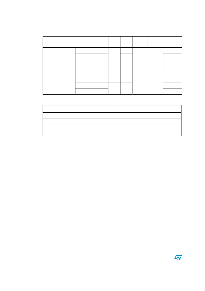
�Table� 17.�
�Port� bit� configuration� table�
�Configuration� mode�
�CNF1�
�CNF0�
�MODE1�
�MODE0�
�PxODR�
�register�
�General� purpose�
�output�
�Alternate� Function�
�output�
�Push-pull�
�Open-drain�
�Push-pull�
�Open-drain�
�0�
�1�
�0�
�1�
�0�
�1�
�01�
�10�
�11�
��0� or� 1�
�0� or� 1�
�don’t� care�
�don’t� care�
�Analog� input�
�Input� floating�
�0�
�0�
�1�
�don’t� care�
�don’t� care�
�Input�
�Input� pull-down�
�Input� pull-up�
�1�
�0�
�00�
�0�
�1�
�Table� 18.�
�Output� MODE� bits�
�MODE[1:0]�
�00�
�01�
�10�
�11�
�Meaning�
�Reserved�
�Max.� output� speed� 10� MHz�
�Max.� output� speed� 2� MHz�
�Max.� output� speed� 50� MHz�
�8.1.1�
�8.1.2�
�140/995�
�General-purpose� I/O� (GPIO)�
�During� and� just� after� reset,� the� alternate� functions� are� not� active� and� the� I/O� ports� are�
�configured� in� Input� Floating� mode� (CNFx[1:0]=01b,� MODEx[1:0]=00b).�
�The� JTAG� pins� are� in� input� PU/PD� after� reset:�
�PA15:� JTDI� in� PU�
�PA14:� JTCK� in� PD�
�PA13:� JTMS� in� PU�
�PB4:� JNTRST� in� PU�
�When� configured� as� output,� the� value� written� to� the� Output� Data� register� (GPIOx_ODR)� is�
�output� on� the� I/O� pin.� It� is� possible� to� use� the� output� driver� in� Push-Pull� mode� or� Open-Drain�
�mode� (only� the� N-MOS� is� activated� when� outputting� 0).�
�The� Input� Data� register� (GPIOx_IDR)� captures� the� data� present� on� the� I/O� pin� at� every�
�APB2� clock� cycle.�
�All� GPIO� pins� have� an� internal� weak� pull-up� and� weak� pull-down� which� can� be� activated� or�
�not� when� configured� as� input.�
�Atomic� bit� set� or� reset�
�There� is� no� need� for� the� software� to� disable� interrupts� when� programming� the� GPIOx_ODR�
�at� bit� level:� it� is� possible� to� modify� only� one� or� several� bits� in� a� single� atomic� APB2� write�
�access.� This� is� achieved� by� programming� to� ‘1’� the� Bit� Set/Reset� Register� (GPIOx_BSRR,�
�Doc� ID� 13902� Rev� 9�
�发布紧急采购,3分钟左右您将得到回复。
相关PDF资料
MCBTMPM330
BOARD EVAL TOSHIBA TMPM330 SER
MCIMX25WPDKJ
KIT DEVELOPMENT WINCE IMX25
MCIMX53-START-R
KIT DEVELOPMENT I.MX53
MCM69C432TQ20
IC CAM 1MB 50MHZ 100LQFP
MCP1401T-E/OT
IC MOSFET DRVR INV 500MA SOT23-5
MCP1403T-E/MF
IC MOSFET DRIVER 4.5A DUAL 8DFN
MCP1406-E/SN
IC MOSFET DVR 6A 8SOIC
MCP14628T-E/MF
IC MOSFET DVR 2A SYNC BUCK 8-DFN
相关代理商/技术参数
MCBSTM32EXLU
功能描述:开发板和工具包 - ARM EVAL BOARD + ULINK2 FOR STM32F103ZG
RoHS:否 制造商:Arduino 产品:Development Boards 工具用于评估:ATSAM3X8EA-AU 核心:ARM Cortex M3 接口类型:DAC, ICSP, JTAG, UART, USB 工作电源电压:3.3 V
MCBSTM32EXLU-ED
制造商:ARM Ltd 功能描述:KEIL STM STM32EXL EVAL BOARD
MCBSTM32EXLUME
功能描述:开发板和工具包 - ARM EVAL BOARD + ULINKME FOR STM32F103ZG
RoHS:否 制造商:Arduino 产品:Development Boards 工具用于评估:ATSAM3X8EA-AU 核心:ARM Cortex M3 接口类型:DAC, ICSP, JTAG, UART, USB 工作电源电压:3.3 V
MCBSTM32F200
功能描述:开发板和工具包 - ARM EVAL BOARD FOR STM STM32F207IG
RoHS:否 制造商:Arduino 产品:Development Boards 工具用于评估:ATSAM3X8EA-AU 核心:ARM Cortex M3 接口类型:DAC, ICSP, JTAG, UART, USB 工作电源电压:3.3 V
MCBSTM32F200U
功能描述:开发板和工具包 - ARM EVAL BOARD FOR STM STM32F207IG + ULINK2
RoHS:否 制造商:Arduino 产品:Development Boards 工具用于评估:ATSAM3X8EA-AU 核心:ARM Cortex M3 接口类型:DAC, ICSP, JTAG, UART, USB 工作电源电压:3.3 V
MCBSTM32F200UME
功能描述:开发板和工具包 - ARM EVAL BOARD FOR STM STM32F207IG ULINK-ME
RoHS:否 制造商:Arduino 产品:Development Boards 工具用于评估:ATSAM3X8EA-AU 核心:ARM Cortex M3 接口类型:DAC, ICSP, JTAG, UART, USB 工作电源电压:3.3 V
MCBSTM32F200UME-ED
制造商:ARM Ltd 功能描述:KEIL STM32F207IG EVAL BOARD
MCBSTM32F400
功能描述:开发板和工具包 - ARM EVAL BOARD FOR STM STM32F407IG
RoHS:否 制造商:Arduino 产品:Development Boards 工具用于评估:ATSAM3X8EA-AU 核心:ARM Cortex M3 接口类型:DAC, ICSP, JTAG, UART, USB 工作电源电压:3.3 V